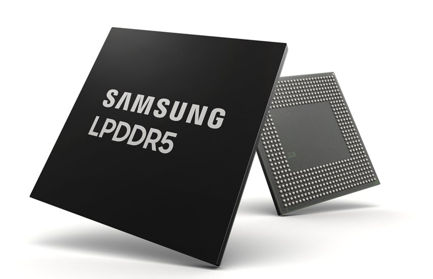
Samsung are the first to announce that they have successfully developed a 10-nanometer class (process node between 10 and 20 nanometers). This announcement is not only ahead of Samsung’s competitors, but also ahead of the finalization of the specifications for DDR5 & LPDDR5. JEDEC, the standards group for the microelectronics industry, is still forecasting the release of the full DDR5 standardsfor later this year. Samsung similarly made their announcement for their LPDDR4 chips ahead of the associated standards in 2014. Since then, they tell us, they have been setting the stage to transition to the LPDDR5 standard for use in upcoming 5G and Artificial Intelligence (AI)-powered mobile applications.
The newly-developed 8Gb LPDDR5 is the latest addition to Samsung’s premium DRAM lineup, which includes 10nm-class 16Gb GDDR6 DRAM (in volume production since December 2017) and 16Gb DDR5 DRAM (developed in February). The 8Gb LPDDR5 boasts a data rate of up to 6,400 megabits per second (Mb/s), which is 1.5 times as fast as the mobile DRAM chips used in current flagship mobile devices (LPDDR4X, 4266Mb/s). With the increased transfer rate, the new LPDDR5 can send 51.2 gigabytes (GB) of data, or approximately 14 full-HD video files (3.7GB each), in a second (assuming a 64-bit memory bus as is common in high-end mobile platforms).
Samsung plans to offer its new LPDDR5 chips in two bandwidths, 6,400Mb/s at a 1.1 operating voltage (V) and 5,500Mb/s at 1.05V. The previous generation LPDDR4x used a similar operating voltage of 1.1V, but only provided a bandwidth of 4,260Mb/s. So the new chips will provide more performance without using more power, and in the case of the lower performance version actually slightly less power. Samsung claims this performance advancement has been made possible through several architectural enhancements. By doubling the number of memory “banks” – subdivisions within a DRAM cell – from eight to 16, the new memory can attain a much higher speed without increased power consumption.
Alongside the architectural improvements to hold down peak power usage, Samsung also has several innovations to reduce average power use. The 10nm-class LPDDR5 has been engineered to lower its voltage in accordance with the operating speed of the corresponding application processor, when in active mode. Additionally, the chip has been configured to avoid overwriting cells with ‘0’ values, thereby avoiding wasting electricity on reiterating an existing value. Most impressively, the new LPDDR5 chip will offer a ‘deep sleep mode’, which cuts the power usage to approximately half the ‘idle mode’ of the current LPDDR4X DRAM. Thanks to these low-power features, Samsung expects to deliver power consumption reductions of up to 30 percent, maximizing mobile device performance and extending the battery life of smartphones.
Samsung has not yet begun mass production. It is possible they’re waiting on the specification to be finalized. They have already selected their factory in Pyeongtaek, Korea as the production site once they being mass production. Given Samsung’s emphasis on mobile applications in their press release, it seems likely that the initial production will be directed towards smartphones and other mobile devices.
Sign up for the StorageReview newsletter

