IBM pioneers an approach to co-packaged optics that leverages light-based connectivity in data centers.
IBM has announced groundbreaking research in optics technology that promises to revolutionize how data centers train and run generative AI models. The company has pioneered a novel approach to co-packaged optics (CPO)—a next-generation technology that leverages light-based connectivity inside data centers. By designing and assembling the first publicly announced polymer optical waveguide (PWG) to power this innovation, IBM researchers aim to redefine how high-bandwidth data is transmitted between chips, circuit boards, and servers.

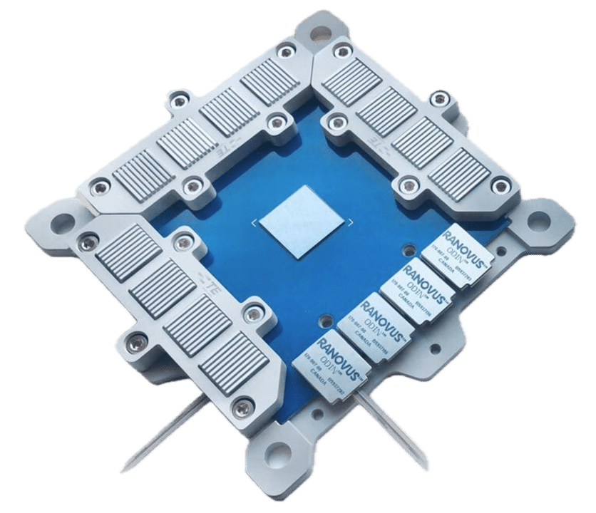
Image courtesy of Ranovus
Fiber optic technology carries vast amounts of data across long distances, managing global commerce and communications. However, within data centers, racks depend on copper-based DAC network cabling for connectivity. IBM feels this setup can create bottlenecks by limiting speed and capacity, leaving GPU accelerators idle for extended periods during distributed AI training processes. IBM’s breakthrough aims to bring the speed and efficiency of optics into these internal connections, dramatically improving performance and energy efficiency.
IBM has demonstrated a new CPO prototype module introducing high-speed optical connectivity within data centers. Published in a paper on arXiv, the research highlights how this technology can drastically increase bandwidth, reduce GPU downtime, and accelerate AI model training while addressing escalating energy demands in data centers.
Key Advantages of Co-Packaged Optics (CPO)
Enhanced Energy Efficiency and Cost Reduction
CPO technology enables a more than 5x reduction in energy consumption compared to mid-range electrical interconnects. This advancement also allows data center interconnect cables to extend from just a few meters to hundreds of meters, reducing operational costs significantly.

- Accelerated AI Training: By replacing traditional electrical wiring with optical connectivity, CPO can increase the speed of training large language models (LLMs) by up to five times. For instance, it can reduce training time for an LLM from three months to three weeks, with even greater performance gains as models and GPU resources scale.
- Unparalleled Energy Savings: IBM estimates that each AI model trained using CPO could save the equivalent of the annual power consumption of 5,000 U.S. homes, underscoring the transformative impact on energy efficiency.
- Unmatched Bandwidth Density: CPO modules offer up to 80 times more bandwidth between chips compared to electrical connections. IBM’s innovation allows chipmakers to add six times more optical fibers at the edge of silicon photonics chips, referred to as “beachfront density,” enhancing overall data center capacity.
Pioneering Polymer Optical Waveguide (PWG) Technology
IBM’s research team designed a high-density PWG with 50-micrometer pitch optical channels adiabatically coupled to silicon photonics waveguides. This assembly, performed using standard packaging processes, is the first to pass stringent manufacturing stress tests, including high humidity, extreme temperatures ranging from -40°C to 125°C, and mechanical durability. Stacking PWGs enables up to 128 connectivity channels, offering unprecedented scalability.

This innovation aligns with IBM’s leadership in semiconductor technology, building on advancements such as the first 2 nm node chip, nanosheet transistors, and vertical transistors (VTFET). CPO technology introduces a new way to meet AI’s increasing demands, transitioning off-module communications from electrical to optical and enabling sustainable and scalable data center operations.
Supporting Generative AI Growth
IBM’s Senior Vice President and Director of Research, Dario Gil, highlighted the transformative potential of CPO:
“As generative AI demands more energy and processing power, the data center must evolve—and co-packaged optics can make these data centers future-proof. With this breakthrough, tomorrow’s chips will communicate much like how fiber optics cables carry data in and out of data centers, ushering in a new era of faster, more sustainable communications that can handle the AI workloads of the future.”

IBM’s work on CPO was conducted in Albany, New York, home to the recently announced National Semiconductor Technology Center (NSTC). Prototype assembly and module testing occurred at IBM’s Bromont, Quebec, facility, a leader in chip packaging. This collaboration is part of the Northeast Semiconductor Corridor initiative, which aims to strengthen semiconductor innovation across the United States and Canada.
IBM’s co-packaged optics innovation represents a significant step forward in advancing data center communications. By integrating light-speed connectivity within racks, CPO technology promises to deliver unparalleled efficiency, bandwidth, and energy savings, redefining data centers’ capabilities and preparing them for the growing demands of generative AI and beyond.
Engage with StorageReview
Newsletter | YouTube | Podcast iTunes/Spotify | Instagram | Twitter | TikTok | RSS Feed
