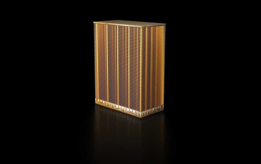
Micron has begun volume production of the world’s first 232-layer NAND, which is highlighted by the industry’s highest areal density. The new 232-layer NAND also offers increased capacity and energy efficiency compared to last-gen Micron NAND, making it ideal for most data-intensive use cases.

Micron 232-layer NAND vs. 176-layer NAND
Micron’s new NAND sets a new industry standard with an I/O speed of 2.4GB/s—a 50% increase in data transfer speeds when compared to the fastest interface enabled on the company’s Micron 176-layer NAND layer node. This makes it ideal for applications that require both low-latency and high-throughput data-centric workloads, including artificial intelligence, machine learning, unstructured databases, real-time analytics, and cloud computing.
Micron 232-layer NAND also claims an improvement of up to 100% for write bandwidth and over 75% in read bandwidth per die, resulting in better performance and energy efficiency in SSDs and embedded NAND solutions.
Moreover, the 232-layer NAND is the industry’s first six-plane TLC production NAND, which features the most planes (each plane having independent read capability) per die of any TLC flash currently available. This combination of I/O speed, read and write latency (along with Micron’s six-plane architecture) makes for fewer collisions between write and read commands. It also promotes system-level quality-of-service improvements.

Another industry first for the 232-layer NAND is support for NV-LPDDR4, a low-voltage interface that Micron quotes as a 30% improvement for per-bit transfer compared to previous I/O interfaces. Micron also says that this 232-layer NAND solution will be able to offer a balance of improved performance with lower power consumption, which means better support for mobile applications, deployments in the data center and at the intelligent edge. The interface is also backward compatible, allowing it to support legacy controllers and systems.
Benefits of Small Form Factor
Because the 232-layer NAND is a compact form factor, customers will have a range of flexible options at their disposal with their designs. This allows it to have an extremely high TLC density per square millimeter (14.6 Gb/mm2). Moreover, Micron indicates that the areal density is 35% to 100% larger than current competing TLC products, which helps minimize board space and enables a diverse range of deployments.
In addition, it ships in new smaller packaging at 11.5mm x 13.5mm, which is 28% less in size compared to previous Micron generations.
Who Really Cares About Layers?
Micron cares a lot obviously, the layers war is a place where they’re leading, so Micron likes to go heavy when it comes to extolling the virtues of their NAND. But end customers don’t really care and no one has made a buying decision based on layer count. What really matters is how all of the technology comes together in a packaged SSD. On that front, Micron has struggled, their SSDs tend to be middling.
But all is not lost, Micron sells their NAND to many other players. In fact, some of the leading client SSDs pair the Phison E18 controller with Micron NAND, and the resulting drives are very good. But ultimately it remains to be seen if all of Micron’s layers and potential advancements in performance translate into good drives out the other side.
Availability
Micron is now shipping the 232-layer NAND to their customers in component form and via the Crucial SSD consumer product line.


 Amazon