

Micron Technology and Intel announced today the availability of their new 3D NAND technology. Jointly developed by both companies, this new flash memory technology is being billed as the world’s highest-density. The companies claim that they will be able to get three times higher capacity than competing NAND technologies.
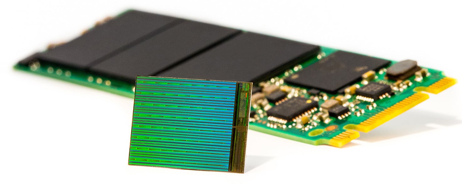
Flash is being adopted into or already used in most fields from consumer mobile devices to enterprise deployments. The largest problem currently facing the industry is that planar NAND is reaching its practical scaling limit. Micron and Intel aim to change this with their 3D NAND that stacks layers of data storage cells vertically.
Intel and Micron chose to use a floating gate cell, which has been used for some time in the industry, in their 3D NAND. This is the first time floating gate cell has been used with 3D NAND. With floating gate cell's proven track record, Intel and Micron believe they can get better performance, reliability, and increased quality from using this technology. This new 3D NAND technology allows flash cells to be stacked vertically in 32 layers. This will achieve MLC dies of 256Gb and TLC dies of 384Gb both of which still fit in a standard package. This increase in capacity will allow M.2 SSDs to achieve a total storage capacity of 3.5TB or more and standard 2.5" SSDs will have a total storage capacity of 10TB or more. This increase in capacity will make flash much more appealing to data centers that need to fit storage within a certain density.
Key features include:
- Large Capacities –Three times the capacity of existing 3D technology—up to 48GB of NAND per die—enabling three-fourths of a terabyte to fit in a single fingertip-sized package.
- Reduced Cost per GB – First-generation 3D NAND is architected to achieve better cost efficiencies than planar NAND.
- Fast – High read/write bandwidth, I/O speeds and random read performance.
- Green – New sleep modes enable low-power use by cutting power to inactive NAND die (even when other die in the same package are active), dropping power consumption significantly in standby mode.
- Smart – Innovative new features improve latency and increase endurance over previous generations, and also make system integration easier.
Availability
The 256Gb MLC is sampling with select partners today and the 384Gb will be sampling later this quarter. Production is expected to start in the second half of 2015.
Toshiba also announced new 3D NAND technology today.


 Amazon