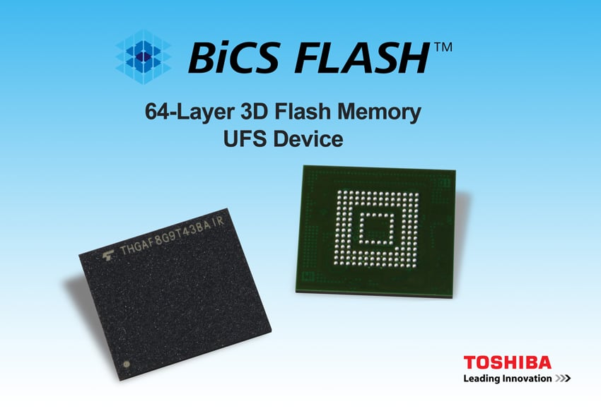
Today Toshiba Memory America, Inc. (TMA) announced that it has began sampling Universal Flash Storage (UFS) devices utilizing its 64-layer BiCS FLASH 3D flash memory. TMA states that these new devices will be able to meet performance demands of applications that demand high-speed read/write performance and low power consumption. Ideal use cases will be in mobile devices such as smartphones and tablets as well as augmented /virtual reality systems.

Toshiba will be releasing four capacities: 32GB, 64GB, 128GB, and 256GB. All of the devices will integrate flash memory and a controller in a single, JEDEC-standard 11.5x13mm package. According to the company, the controller performs error correction, wear leveling, logical-to-physical address translation, and bad-block management – allowing users to simplify system development.
From a performance perspective, Toshiba is claiming numbers of 900MB/s read and 180MB/s write (for the 64GB version). They go on to claim random performance improvements of 200% and 185% read and write over previous generations though don’t give numbers. The new devices are also JEDEC UFS Ver. 2.1 compliant (including HS-GEAR3), giving them a theoretical interface speed of up to 5.8Gbps per lane (x2 lanes=11.6Gbps) while also suppressing any increase in power consumption. The new UFS devices support full duplexing through their serial interface, meaning they can concurrently read and write between the host processor and UFS device.


 Amazon